
- Table of Contents
- Day 1
- Day 2
- Day 3 RISC - V core Programming on Vivado
- Day 4 - SOFA FPGA Fabric IP
- Day 5 SOFA RISC - V Core
- Acknowledgements

We shall be looking at a 4-bit counter example and the RISC-V RVMyth Processor through two flows:
- Vivado
- Skywater OpenSource FPGA (SOFA)
Programmable Logic Devices.
- The hardware can be customized after the manufacturing by programming the device
- PLA - Produces Minterms, Variable AND Gates, Input to OR Gates is fixed. But sequential elements cannot be programmed using this
- CPLD - Complex Programmable Logic Devices
- FPGA - Field Programmable Gate Arrays
FPGA consists of Lookup Tables, Flip Flops and CLBs (Configurable Logic Blocks)
| ASIC | FPGA |
|---|---|
| Not programmable | Reprogrammable |
| Final Stage implementation | Useful in prototyping a design |
| Huge time required to design | Less Time Comparatively |
| RTL to Layout | RTL to Bitstream generation |
- FPGAs are good for implementing algorithms which are able to run parallely.
- Hardware acceleration implementation of Neural Networks.
- Embedded Systems
- Machine Learning
- Can be used to implement any combinatorial and sequential design.

(Diagram taken from Course Slide for reference)
An FPGA Architecture consists of
-
Configurable Logic Blocks
- It contains an N-input Lookup Tables, Carry chain, Multiplexer and a Flip Flop.
-
Programmable Interconnects
- The wires which connect the CLBs.
-
Programmable I/O
- User generates a bitstream for their design specification, and uploads it into the board.
- Bitstream describes what CLBs that have to be connected and their function.
- It also defines the connection between the CLBs and I/Os.
- The Lookup table consists of all the possible minterms of a N-input function.
- Basically a function can be expressed as Sum of Products form or Sum of Minterms form.
- If we want to implement a logic function, the corresponding minterms of the function are selected by using the Mux.
- The output of the Mux feeds into the Flip Flop.
- A
$2^N$ - input Mux can be used to implement any N - input Function or some N + 1 input function with an additional NOT gate.
- HDL - Verilog
- HLS - C/C++/Python
graph TD;
  A[Architectural Description] --> B[RTL Design and testbench]
  B --> C[Behavioral Simulation]
  C --> D["Synthesis (Timing Analysis)"]
  D --> E["Implementation Place/Route (Timing Analysis)"]
  E --> F[Bitstream generation]
  F --> G[FPGA Programming]

  H[Timing constraints] --> D
  I[Pin Assignments] --> D
The following are non-synthesizable:
- User defined delays
- Inital block
- nmos, pmos primitives
- Dynamic Memory allocation
- Infinite loops
 (Image taken from slide for reference)
- Xilinx Vivado 2019.2 - https://www.xilinx.com/support/download/index.html/content/xilinx/en/downloadNav/vivado-design-tools/archive.html
- Local Programming using a board
- Remote Programming - A FPGA connected to a remote server: I/O through Virtual I/O.
- We use a frequency synthesizer to generate a slow clock to observe the outputs
Code
module counter(clk,reset,count);
input clk,reset;
output reg [3:0] count = 4'b0000;
reg [25:0] count_reg;
reg clk_div = 1'b0;

always @ (posedge clk)
begin
if (reset)
    begin
        clk_div <= 1'b0;
        count_reg <= 26'd0;
        ///count <= 4'b0;
     end
else
    begin
        count_reg <= count_reg + 1;
    /// if (count_reg == 26'h3ffffff) // for synthesis
        if (count_reg == 26'd12) // for simulation
        begin
            clk_div <= ~ clk_div;
            count_reg <= 26'd0;
        end
    end
 end

  always @ (posedge clk_div) begin
   if (reset)
   begin
      count <= 4'b0000;
   end
   else
   begin
      count <= count + 1'b1;
   end
  end
endmodulei. Type vivado in the terminal.
ii. Create a new project.
iii. Do the following settings.

iv. Click finish.
v. Add source files
- Set the testbench as top module while during Behavioural Simulation
vi. Run Behavioural Simulation

- The output counter gets incremented at every posedge of the slow clock
vii. Now set the design as top unit (not the testbench)
vii. Run Elaboration

viii. Do the I/O pin assignment as follows and save as constraints.xdc file.


- The data should be available Tsetup before the capturing clock edge comes.
- We need fast cells to satisfy Max Delay constraints.
- Setup time constraints are always calculated with respect to the next clock edge.

- Data should be stable for T-hold after the clock edge to be captured properly.
- If the next data comes earlier than T-hold, the current data will not be captured properly.
- We need slow cells to satisfy hold time constraints
- Setup slack = Required Arrival Time(Clock setup time) - Arrival Time (Data)
- Delay in clock helps us
- Delay in data is not feasible here
- Hold Slack = Arrival Time(Data) - Required Arrival Time(hold time of FF)
- Here delay in data is helpful
- But delay in clock is not desirable.
i. Now run synthesis.

ii. Primary clock is selected.

iii. No generated clock.
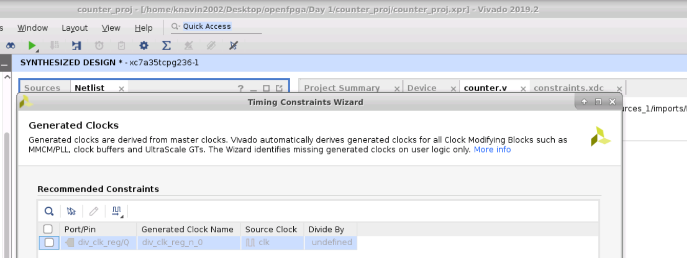
iv Skip to finish.

v. Synthesized netlist


- Click program device to send the bitstream to the FPGA board.
This can be done after synthesis or after implementation.
i. Click on Report Timing Summary

ii. We can also view the detailed path report for each path. It specifies the starting and endpoint.

- As the slack is positive, all the timing constraints are met.

- Click on report Resource Utilization

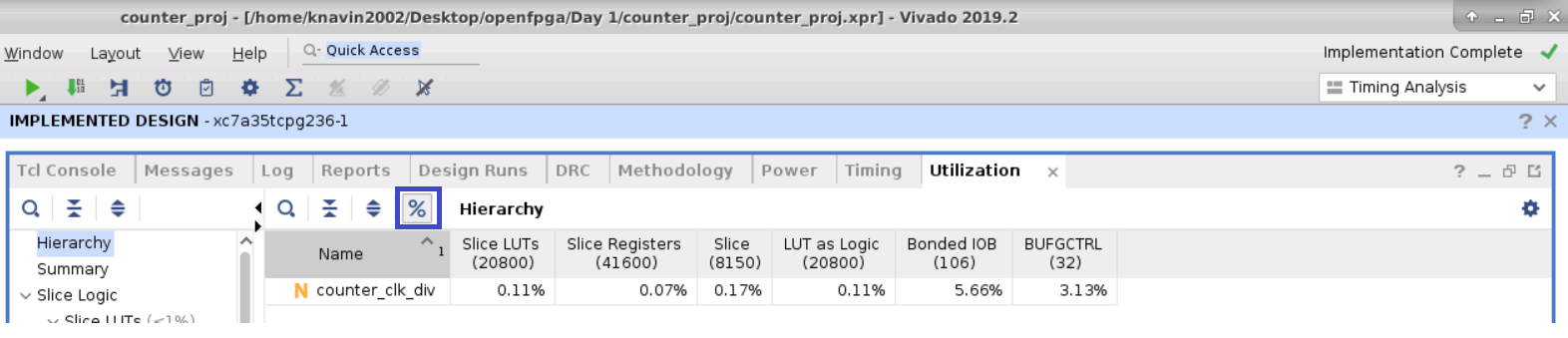
- Summary

- Using this method we can program a remote FPGA connected to a cloud.
- The VIO provides the inputs to the FPGA and probes the output.
- VIO output is the input to the FPGA
- VIO input is the output of the FPGA

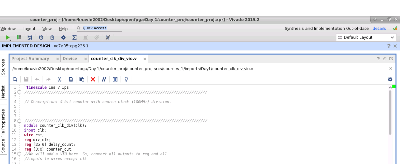
- Make these changes. The reset and clock are come from VIO. So they are no longer input ports. The counter output will be probed by the VIO, so it is no longer an output port.
VIO Inputs: Slow Clock, Counter Output VIO Outputs: Reset
i. Click on IP Catalog in the Project Manager.
ii. Search VIO

iii. Configure as shown.


iv. Click generate
v. Go to IP Sources and click on Instantion Template and copy these lines from the .veo file.

vi. Use this to instantiate the VIO in the .v file


- It is an open source framework to quickly generated a custom FPGA fabric specific to our design
- It is automated
- Reduces development time
- Generally it takes 24 hours to produce a production ready layouts
- For certain applications custom-made FPGAs provide huge performance gain.
- Custom FPGA architectures are expensive to produce
- OpenFPGA allows us to customize our own FPGA fabrix using a set of templates
- Generate verilog netlists based on an XML file - VPR ( Versatile Place and Route )
- Automatically generates Verilog testbenches'
- Bitstream generation based on XML format
Visit this repo to install OpenFPGA: https://github.com/lnis-uofu/OpenFPGA
-
XML - based architecture description language to describe the custom FPGA architecture
-
Download Link: https://github.com/verilog-to-routing/vtr-verilog-to-routing
-
Documentation: https://docs.verilogtorouting.org
-
Basically it maps our RTL to a placed and routed FPGA
graph TD;
  A[Verilog Digital Circuit] --> E["Elaboration & Synthesis (Odin II)"]
  B[XML FPGA Architecture] --> E
  E --> L
  L["Logic Optimization & Technology Mapping (ABC)"] --> P["Pack the netlist, Placement, Routing and Timing Analysis (VPR)"]

  P --> O[Output Statistics]
  P --> PI[Post-Implementation netlist]
i. We shall first run VPR on a Pre-synthesized circuit. ii. Then, we shall run entire VPR Flow from RTL
i. Packing - combines the technology mapped netlist into (CLBs) Complex Logic Blocks. ii. Placement - postition of the CLBs - it produces a .place file. iii. Routing - interconnection between blocks iv. Analysis - Analyzes the implementation
Input: Blif file, Earch
This is the general structure of a Earch.xml file. It describes the FPGA Architecture.
<!--
-->
<architecture>
  <models>
    <model name = "">
    </model>
  </models>
  <tiles>
    <tile name = "">
    </tile>
  </tiles>
  <layout> <!-- Grid Layout, aspect ratio -->
  </layout>
  <device> <!-- Transistor definitions -->
  </device>

  <switchlist>
  </switchlist>

  <segmentlist>
  </segmentlist>

  <directlist>
  </directlist>

</architecture>.names - LUTS
i. Create a working directory.
mkdir -p vtr_work/quickstart/vpr_tseng
cd ./vtr_work/quickstart/vpr_tseng
ii. Now pass the FPGA architecture and the technology mapped netlist of the design.
$VTR_ROOT/vpr/vpr \
$VTR_ROOT/vtr_flow/arch/timing/EArch.xml \
$VTR_ROOT/vtr_flow/benchmarks/blif/tseng.blif \
--route_chan_width 100
--disp on


iii. Additional parameter can be applied here
$VTR_ROOT/vpr/vpr \
$VTR_ROOT/vtr_flow/arch/timing/EArch.xml \
$VTR_ROOT/vtr_flow/benchmarks/blif/tseng.blif \
--route_chan_width 100
--analysis
--disp on
- .net file: post packed circuit, circuit in terms of CLBs.
- .place file: how the cells are placed
- .route file: interconnects
- .log file:

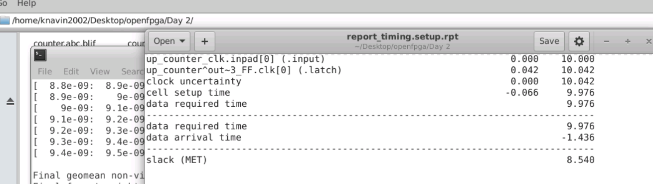
- Here, the setup slack is violated as no clock constraints are specified.

i. Create a tseng.sdc file
create_clock -period 10 -name pclk
set_input_delay -clock pclk -max 0 [get_ports {*}]
set_output_delay -clock pclk -max 0 [get_ports {*}]
ii. Run include sdc file as part of the command
$VTR_ROOT/vtr_flow/arch/timing/EArch.xml $VTR_ROOT/vtr_flow/benchmarks/blif/tseng.blif --route_chan_width 100 --disp on --sdc_file tseng.sdc- Now we can see that the setup slack is met.

i. Run the automated VTR Flow command.
$VTR_ROOT/vtr_flow/scripts/run_vtr_flow.py \
      /home/knavin2002/Desktop/openfpga/Day\ 2/vtr_work/counter.v \
      $VTR_ROOT/vtr_flow/arch/timing/EArch.xml \
      -temp_dir . --route_chan_width 100

ii. We can run vpr (flow analysis) on the pre-vpr file.blif file.
$VTR_ROOT/vpr/vpr $VTR_ROOT/vtr_flow/arch/timing/EArch.xml \
                  counter --circuit_file counter.pre-vpr.blif \
                  --route_chan_width 100 \
                  --analysis --disp on
iii. Now run the entire VPR Flow
$VTR_ROOT/vpr/vpr $VTR_ROOT/vtr_flow/arch/timing/EArch.xml \
                  counter --circuit_file counter.pre-vpr.blif \
                  --route_chan_width 100 --disp on

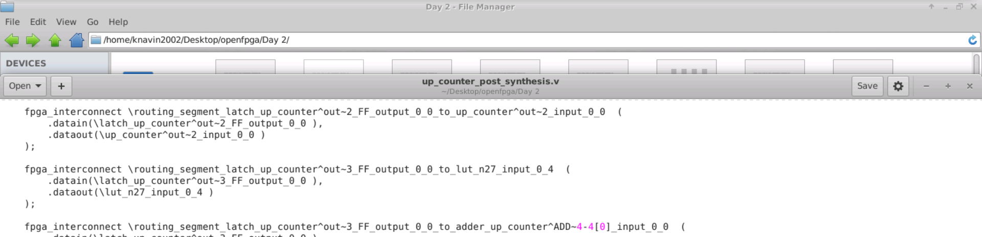
iv. Generation of Post implementation netlist
$VTR_ROOT/vpr/vpr $VTR_ROOT/vtr_flow/arch/timing/EArch.xml \
                  counter.pre-vpr.blif \
                  --gen_post_synthesis_netlist on

- To run the post implementation netlist, we need primitves file
v. Simulation in Xilinx Vivaldo. Include post_synthesis file, testbench and primitives file

- Include the path to the .sdf file correctly in the testbench.


- We have to pass the
.blifto the VPR Flow otherwise the tool will have its own constraints.
i. Create a constraints.sdc file. Create constraints as follows. Also change the name of the clock in the pre-vpr.blif as up_counter_clk.
create_clock -period 10 up_counter_clk
set_input_delay -clock up_counter_clk -max 0 [get_ports {*}]
set_output_delay -clock up_counter_clk -max 0 [get_ports {*}]
ii. Now run VPR flow with te timing constraints.
  $VTR_ROOT/vpr/vpr \
  $VTR_ROOT/vtr_flow/arch/timing/EArch.xml \
  counter.pre-vpr.blif --route_chan_width 100 \
  --sdc_file /home/knavin2002/Desktop/openfpga/Day\ 2/tseng.sdc
iii. We can check whether the setup and hold time constraints are met.
iv. Now change the clock period to 5ns in .sdc file.

v. Check the setup and hold constraints.


- They are still met.
i. Open vpr_stdout.log file.


i. Include the -power and the cmos_tech xml file the vtr flow command.
  $VTR_ROOT/vtr_flow/scripts/run_vtr_flow.py \
  /home/knavin2002/Desktop/openfpga/Day\ 2/vtr_work/counter.v \
  $VTR_ROOT/vtr_flow/arch/timing/EArch.xml -power -cmos_tech \
  $VTR_ROOT/vtr_flow/tech/PTM_45nm/45nm.xml \
  -temp_dir . --route_chan_width 100

- Now we shall consolidating all the results from the Vivado flow and the VTR Flow of the counter design.
.sdcfile- Clock period
10nsor100 MHz
| Parameter | Basys3 | VTR Earch |
|---|---|---|
| Technology | 28 nm | 40 nm |
| Worst Negative Slack - Setup | 5.77 ns | 8.54 ns |
| Worst Negative Slack - Hold | 0.23 ns | 0.293 ns |
- Minimum Slack
| Parameter | Basys3 (ns) | VTR Earch (ns) |
|---|---|---|
| Minimum Time Period | 3.5 | 1.8 |
| Worst Negative Slack - Setup | 0.41 | 0.34 |
| Worst Negative Slack - Hold | 0.33 | 0.293 |
| Parameter | Basys3 | VTR Earch (ns) |
|---|---|---|
| LUTs | 23 | 18 |
| I/O | 6 | 7 |
| Flip Flops | 31 | 4 |
| Parameter | Basys3 | VTR Earch (ns) |
|---|---|---|
| Clocks | 1e-3 | 1e-4 |
| Signals | 1e-3 | 1.4e-5 |
| Logic | 1e-3 | 8.2e-5 |
| I/O | 1.1e-2 | 0 |
| Dynamic | 1.2e-2 |
- Now we shall go through the Vivado flow for the RVMyth Processor
- RISC - V RVMyth: https://github.com/NAvi349/riscv-myth-ws
- Converting TL - Verilog to Verilog: https://github.com/NAvi349/mixed-riscv-soc
- We shall test a program that sums numbers from 1 to N.
- N is 9 for this example.
$Sumof(1 to 9) = 45$
i. Create a new project and add the core as a source and add a testbench as simulation source.
ii. Run Behavioural Simulation.

- We can see the output is 45 as expected.
i. Assign pin number as shown.

ii. We shall use ILA to observer the outputs. So remove the output ports and declare it as reg.

iii. Run Elaboration again

iv. From IP Catalog instantiate ILA and connect to the RISC - V core

v. Run Synthesis and then add constraints

vi. Run synthesis


i. Run implementation.

ii. Report timing summary

- All the user constraints are met.
i. Run Bitstream generation.


- SOFA - Skywate Opensource FPGAs
- Open-source FPGA IPs
- Skywater 130nm PDK and OpenFPGA Framework
- HD - High Density FPGAs - embedded FPGAs.
- Documentation and installation: https://github.com/lnis-uofu/SOFA
i. Clone the repository
git clone https://github.com/lnis-uofu/SOFA.gitii. Make FPGA1212_QLSOFA_HD_PNR/ as the current directory.
iii. Copy the counter.v file to the benchmark folder.

iii. Open task_simulation.conf
gedit FPGA1212_QLSOFA_HD_task/config/task_simulation.conf
iv. Add the following lines under respective sections
[BENCHMARKS]
bench0=${PATH:TASK_DIR}/BENCHMARK/counter_new/counter.v

[SYNTHESIS_PARAM]
bench0_top = up_counter

generate_testbench.openfpgawill call the vpr flow

- architecture is available under
archdirectory.

v. Run the makefile
make runOpenFPGA
vi. View the generated files
cd FPGA1212_QLSOFA_HD_task/latest/vpr_arch/up_counter/MIN_ROUTE_CHAN_WIDTH/


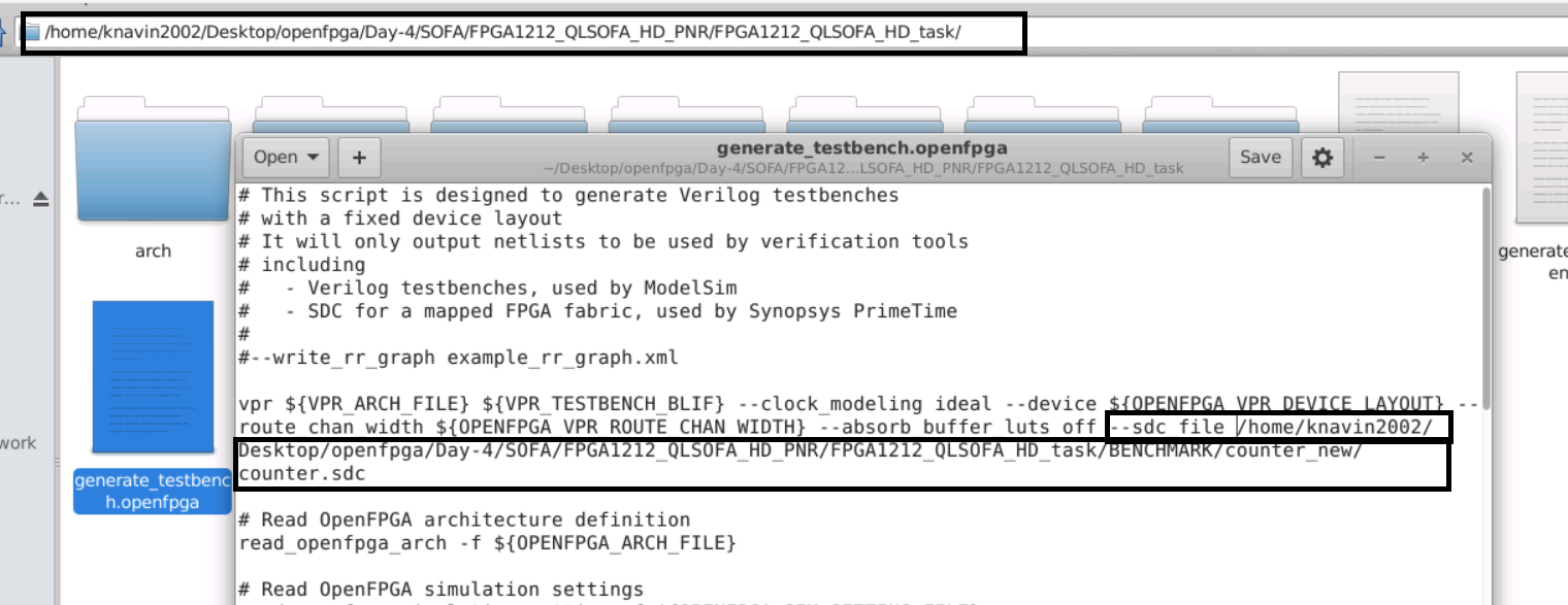
i. Create counter.sdc file in the counter_new folder in BENCHMARK.
create_clock -period 20 clk
set_input_delay -clock clk -max 0 [get_ports {*}]
set_output_delay -clock clk -max 0 [get_ports {*}]
ii. Open generate_testbench.openfpga and the counter.sdc file in the vpr arguments.
iii. Run the makefile command
make runOpenFPGA
- Setup slack

- Hold Slack

i. Add this argument in the vpr flow in the generate_testbench.openfpga file.
--gen_post_synthesis_netlist on
ii. Run makefile again

- post implementation file

iii. Run simulation through vivado.

i. Change this two lines in the task_simulation.conf file.

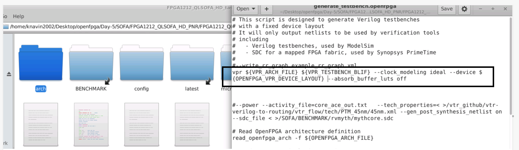
ii. Add this new line the generate_testbench.openfpga file
vpr ${VPR_ARCH_FILE} ${VPR_TESTBENCH_BLIF} --clock_modeling ideal \
  --device ${OPENFPGA_VPR_DEVICE_LAYOUT} --route_chan_width ${OPENFPGA_VPR_ROUTE_CHAN_WIDTH} \
  --absorb_buffer_luts off --power \
  --activity_file /home/knavin2002/Desktop/openfpga/Day-4/SOFA/FPGA1212_QLSOFA_HD_PNR/FPGA1212_QLSOFA_HD_task/latest/vpr_arch/up_counter/MIN_ROUTE_CHAN_WIDTH/up_counter_ace_out.act \
  --tech_properties /home/kunalg123/Desktop/vtr-verilog-to-routing/vtr_flow/tech/PTM_45nm/45nm.xml
iii. Add the options for power analysis in vpr_arch.xml file.
<!-- added for power analysis  -->
  <power>
      <local_interconnect C_wire="2.5e-10"/>
      <mux_transistor_size mux_transistor_size="3"/>
      <FF_size FF_size="4"/>
      <LUT_transistor_size LUT_transistor_size="4"/>
  </power>
  <clocks>
    <clock buffer_size="auto" C_wire="2.5e-10"/>
  </clocks>
iv. Run the makefile command again.

v. See the output in counter.power.

- We shall fall the same steps for the RISC - V RVMyth Core
i. Git clone the SOFA repo as before.
ii. Make these changes in the corresponding files. Also refer to the files in the Day 5 folder. Comment lines 157 and 158, line 259 in the vpr.xml.


iii. Run makefile command

iv. Open openfpgashell.log.

- Open
vpr_stdout.logfor the output statistics.

- Logic Elements

i. Create .sdc file
create_clock -period 200 clk
set_input_delay -clock clk -max 0 [get_ports {*}]
set_output_delay -clock clk -max 0 [get_ports {*}]
ii. Pass the .sdc file as argument in generate_testbench.openfpga


iii. Run the makefile command.
- Setup slack

- Hold slack

i. Add the required argument.

ii. Run makefile

iii. View the core_post_synthesis.v

- Check the waveform using Vivado simulation. It is correct (45 = Sum of 1 to 9).

- Kunal Ghosh, Founder, VSD
- Nandita Rao, Course Instructor
- Dr. Xifan Tang, OpenFPGA and Chief Engineer RapidSilicon