-
Notifications
You must be signed in to change notification settings - Fork 62
Vinyl Cut PCBs
The lalboard was designed to use 3D printed pcb bases that have copper traces that are cut out of adhesive-backed copper tape via a vinyl cutter.
The PCBs should be printed out of a relatively heat resistant plastic, like PC or ABS, so that the brief heat from soldering doesn't melt them (much).
The designs for the vinyl cut traces are in the svg files in the "vinyl_cut_pcb" directory. They all have multiple layers of copper traces, which are insulated from each other as needed by "normal" vinyl, like is normally used with a vinyl cutter. There are typically 3 layers in the SVG for each layer of traces. A "path", "stroke" and "cut" layer. In some cases one or more of these may be omitted.
- The "path" layer is where the traces are actually laid out. It has paths with a very wide stoke width connecting the various solder pads.
- The "stroke" layer takes the paths from the previous layer, and converts the path stroke to shapes via inkscape's "Path->Stroke to Path" functionality, and then those shapes are merged with the solder pads to form a single outline. In some cases, the resulting outlines are tweaked. E.g. by smoothing over very small features that are not needed that can cause problems when cutting
- The "cut" layer is the final result that is actually exported to hpgl and cut. The cut layer takes the outlines from the stroke layer, adds a break somewhere, and adds intro and outro lines at the break, to help facilitate cutting. This isn't always needed, but it can be helpful for problematic cuts. Sometimes the intro/outro will extend all the way to the border, which can break up the waste copper so it can be removed in smaller sections.
In some cases, there is no "cut" layer, in which case the stroke layer should be used to perform the cut instead.
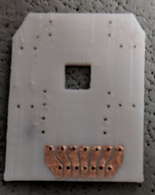
On the thumb cluster pcbs and the main finger cluster pcbs, there are 2 layers of copper on the bottom of the PCB, and 1 layer on the top. The top traces are needed to connect the JST connector back down to the bottom of the PCB.
- The top of the printed part will typically be a bit rough. I like to take a razor blade and scrape it over the top to trim off any little bits of plastic that are sticking up.
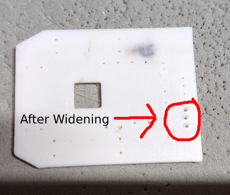
- Next, I take the fine beading awl and stick it through all of the holes, to make sure they are nice and open. Ideally you want them big enough that it's not too difficult to push the LED/connector leg in, but small enough that the leg won't just fall out. This also deforms the plastic and makes a little ridge around the hole, which will make it easier to see the hole once covered by the copper trace.
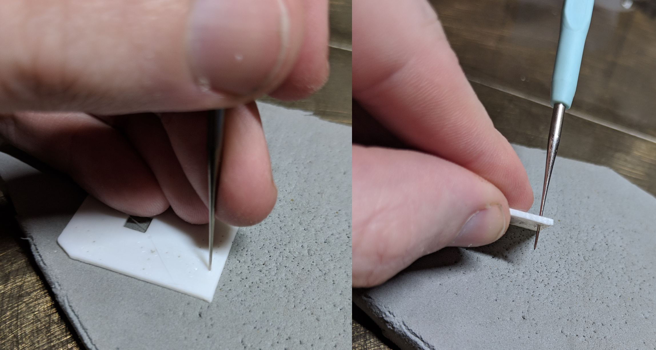
One of the critical aspects of cutting the traces is making sure the blade in the vinyl cutter is set correctly. A 45 degree cutter works well, and you want to set it so that it's just barely poking out of the blade holder - just barely enough to cut through the copper. If it's sticking out too much, it can cause the copper to lift up while cutting, especially at the ends of traces, or other small features.
Also, you should set the cutting force much lower than is typically used for vinyl. On my US Cutter brand vinyl cutter, I typically have it set to 80-90g for cutting vinyl, but I only use 40g for cutting the copper. I also set it at the slowest speed setting, 4in/s.
Once you have it set up, use the top-most layer for a given trace in the SVG file to actually perform the cut. There will typically be a "cut" layer, but if not, use the "stroke" layer.
Perform the cut as you normally would. For my US Cutter cutter, I export the relevant layer as an .hpgl file directly from inkscape, and simply cat it to the serial port of the cutter. e.g. "cat layer1.hpgl > /dev/ttyUSB0".
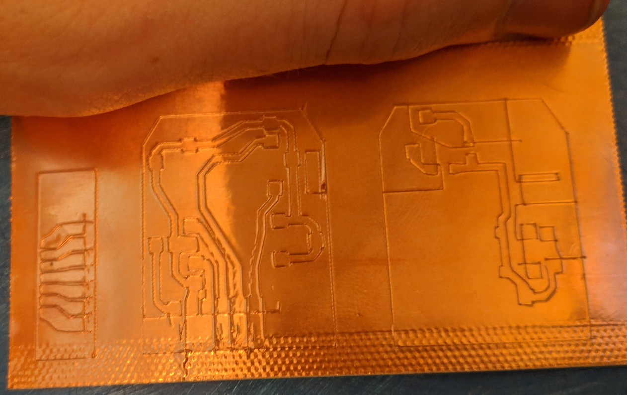
Once cut, you need to remove all of the unwanted copper. This can sometimes be a bit difficult, and might take some practice. Just take it slow and watch for any traces that start to lift up. You can use some tweezers, etc. to hold the trace down while removing the waste copper. It's usually better to try and remove small sections of the waste copper at a time, tearing the excess copper off when needed.
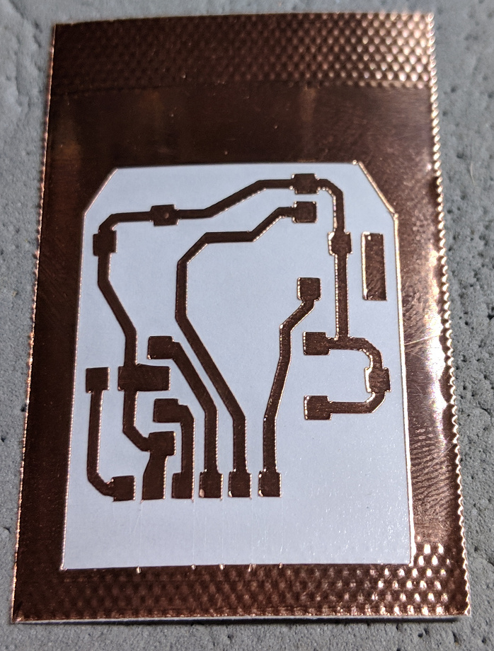
Also, it's best to leave the copper that's outside of the PCB outline. This serves as a good visual aid for getting the traces aligned correctly when placing them onto the printed PCB.
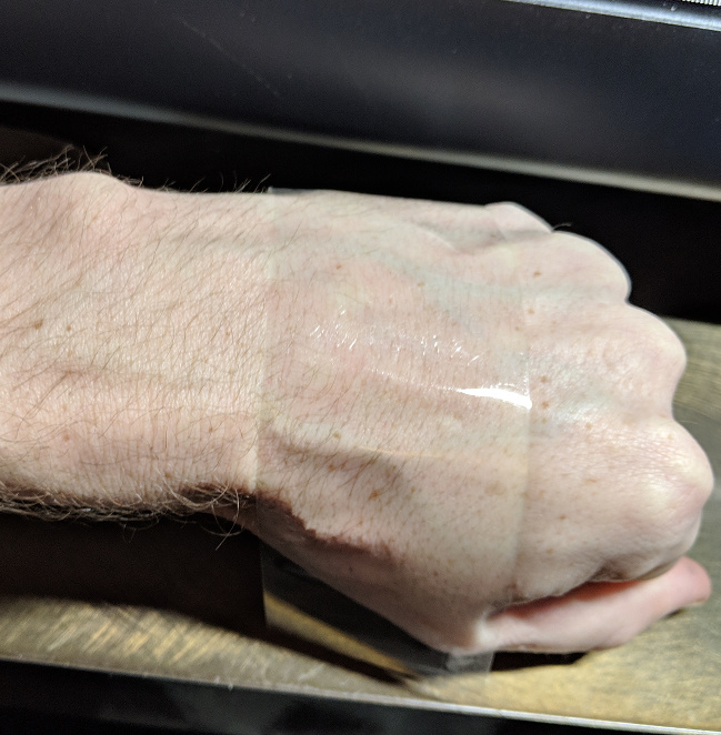
To apply the traces, you can use clear packing tape as a transfer tape. Depending on the tape you have, you may need to reduce the stickiness of the tape, so it doesn't try to pull up the traces after applying them. I do this by first putting the tape on the back of my hand and pressing firmly.
Next, apply the tape to the top of the weeded copper traces.
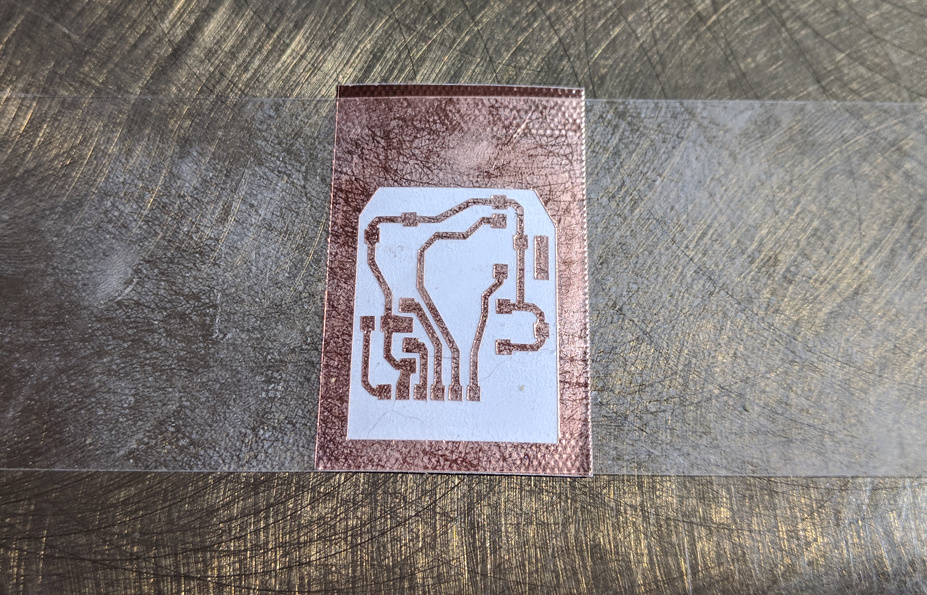
Now, carefully peel off the backing from the copper tape, and make sure all the traces and the outer copper remain stuck on the transfer tape.
Secure the pcb so that it won't move, and then grab the tape at either end, pulling it somewhat tight, and visually line up the outline of the outer copper with the edges of the PCB. You want to get this lined up as perfectly as possible, so that the holes in the PCB will properly line up with the corresponding copper pads.
If the outline of the copper doesn't seem to quite match up with the printed part, you may need to tweak the size of the svg to correct for your printer's resolution. If you're exporting an .hpgl from inkscape, you can also tweak the resolution during the export. The resolution is normally 1016x1016, but I had to reduce it to 992x1000 for my cutter, to get the right cut sizes.
Note: most traces should be applied on the bottom of the printed PCB - the side that was on the print bed. However, the "top" traces should be applied on the opposite side.
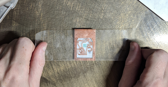
Once you have the tape with the traces stuck down, use the back of your fingernail to rub down on the traces, to make sure they are adhered well. Then, carefully start peeling up the transfer tape, making sure that no traces come up with it.
Once you've applied all the traces on one side, you can use the needle awl to poke through copper trace where there are holes in the PCB. If you've pressed the traces down firmly with the back of your fingernail, you can usually see an imprint of the hole underneath it. If not, you can guestimate where the hole is, or carefully poke through the copper from the other side. Just be aware that this may lift up the copper trace.
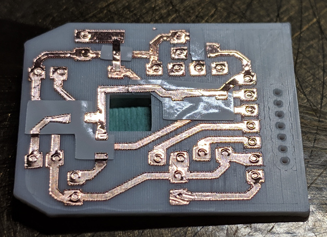
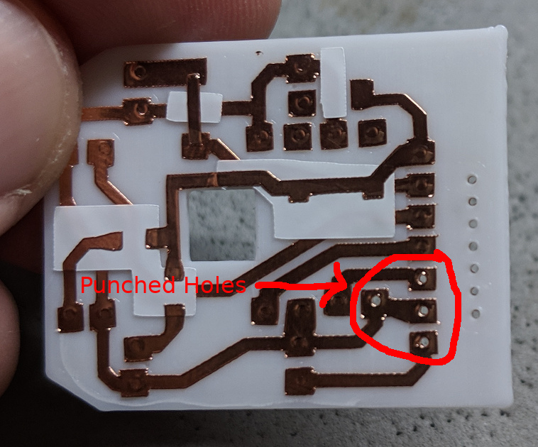
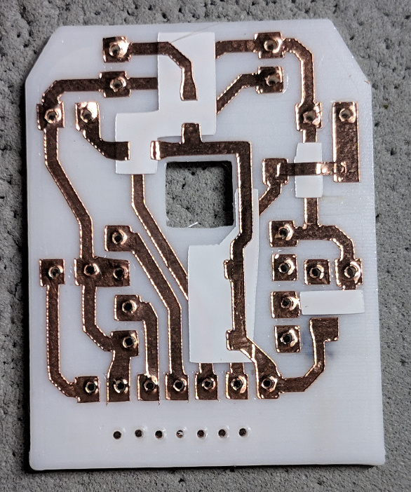
And here is the finished pcb for the main finger cluster
